


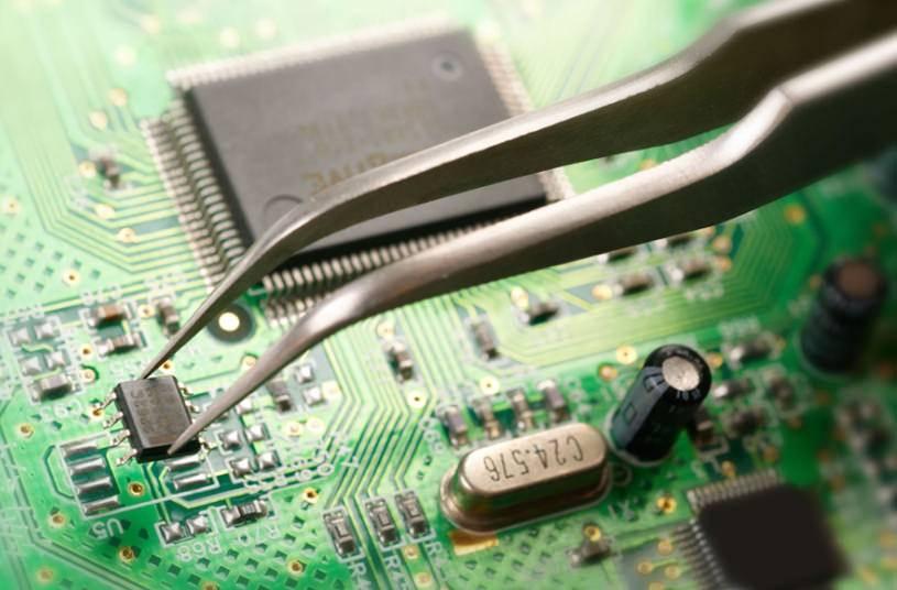
Previously, it was difficult to track the cost of circuit board rework because labor, equipment, and WIP in the rework process were not expensive and could be “swept under the table.” With today’s brand-new and intricate packages, rework has begun taking on a completely new meaning. The necessary equipment, training, and engineering support cost electronic assemblers millions of dollars, not to mention the damage/scrap generated. To replace defective components, expert personnel must use manual techniques and appropriate equipment; area array packages, such as ball grid array (BGA) devices, require special expertise and tools.
In addition to physical damage, component failure is the most obvious cause of PCB repair and rework. Component failure may be caused by poor component quality, element dislodging, or element aging. The most common cause, however, is poor PCB layout. A poor design may result in power failings, overheated parts, and burnt-down components. As a result, it is critical to monitor the circuit board rework process.
The complete step-by-step guide –
- Visual inspections —
A visual inspection can reveal a lot. The best and simplest to detect are burned or eroded components, which indicate overheating or contaminant fluid leakage as factors that cause the malfunction. You can also see missing parts indicating a faulty board. Finally, clear away any debris before probing the board further for problems.
- When it comes to the circuit board rework process,- To guarantee a smooth PCB rework and bring improvement, it is critical to understand the materials used in its manufacture and common problems with your specific board where the board was created.
- Physical inspections — A physical examination may provide additional information when the board is loaded. An oscilloscope can also detect impedance problems created by age-related power difficulties.
- Test the integrity of battery packs, circuitry, resistors, diodes, switches, and transistors by delving deeper into the PCB’s many components.
- Integrated circuit testing — Testing integrated circuits is the final stage of PCB troubleshooting (ICs). An oscilloscope is also useful in this situation. The best method is to locate a known brand circuit and compare all ICs to it to identify problematic ones.
- The circuit board rework procedure is the same whether eutectic or Pb-free solder is used. It starts with a thorough thermal profile, removing failed elements, cleaning and getting ready the site, and attempting to remove rust or solder residues. The component is then replaced with fresh flux and solder, reflowed, and finally inspected.
Rectification and restoration will be much easier with this knowledge. Rework (or re-work) is the word used to describe the refinishing or repair of an electronic printed circuit board (PCB) assembly. This process often entails re-soldering and desoldering of surface-mounted electrical components (SMD). Single device repair or replacement is ineligible for mass processing techniques.
Area array packages, such as ball grid array (BGA) devices, call for specialist knowledge and skills, as well as highly specialized manual processes carried out by skilled employees utilizing the right equipment. The use of a hot air gun or hot air station to heat objects and melt solder is common. Specialized equipment is required to pick up and often put small components.
Reflowing is a rework technique that involves disassembling the apparatus to consider removing the defective circuit board, preheating the entire board in an oven, heating the malfunctioning element further to melt the solder, then attempting to cool, going to follow a series of strategic thermal profiles, and reassembling. It is hoped that this process will fix the loose connection without removing and replacing the element. This could or might not fix the issue, and there’s a chance that the reflowed board will malfunction once more after some time.
Lifted pads, disturbing solder interconnection adjacent to the BGA rework area, solder balls in under stocked or conformably coated areas, and component warping are the most common PCB defects to avoid.
The following are the basic requirements for this operation:
- Heat the entire PCB to 75º C and 125ºC.
- Ensure all joints’ temperature is greater than 190ºC (230ºC for lead-free).
- Ensure that the temperature of all joints is less than 220ºC.
- Assure that no solder is smudged on the part’s bottom or edge, as this may aid in component restoration.
- Maintain adjacent element temperature changes below 180ºC (200ºC for lead-free) to reduce heat influence on these parts.
CONCLUSION
Due to base material damage, valuable circuits are frequently scrapped. Circuits to base material damage, on the other hand, can be fixed reliably. There are numerous well-established circuit board rework processes for trying to repair base material damage caused by various causes. Chipping burns from overheated elements and disoriented capacitors are all instances of damage. Damage can happen during re-work, such as debonding and measling, induced by overheating the board with a heating element or a hot air tool. It can also result from board design errors that necessitate resetting a design and manufacturing a hole or alignment slot. But it is necessary to choose the right person or institution to ensure the work is error-less and free from any further need for adjustments.